Essential Tips For Implementing Jlcpcb Design Rules Altium And Kicad Jlcpcb Design Rules In Your Next Project - Stm32 pcb design
If you are looking for KiCad 8 Custom PCB Design Rules | SaludPCB you've visit to the right place. We have 35 Pictures about KiCad 8 Custom PCB Design Rules | SaludPCB like KiCad-DesignRules/JLCPCB/JLCPCB.kicad_dru at main · labtroll/KiCad, KiCAD-Custom-DRC-Rules-for-JLCPCB-with-Unit-Tests/JLCPCB Rules Test and also STM32 PCB Design - Complete Walkthrough - Altium Designer & JLCPCB. Here it is:
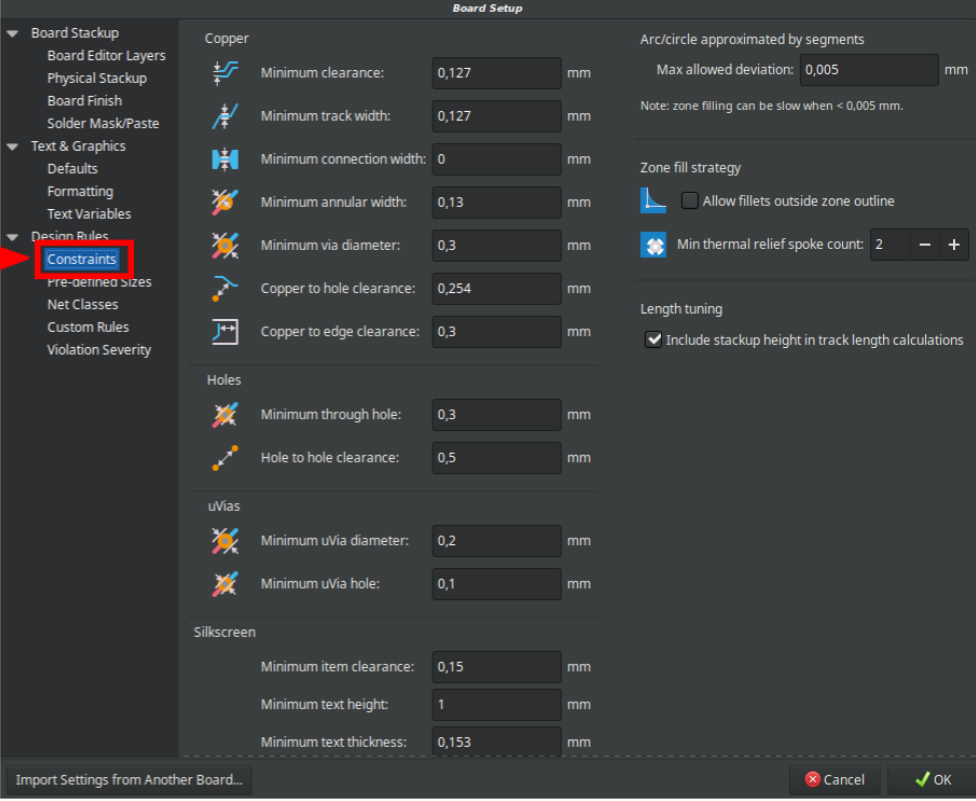
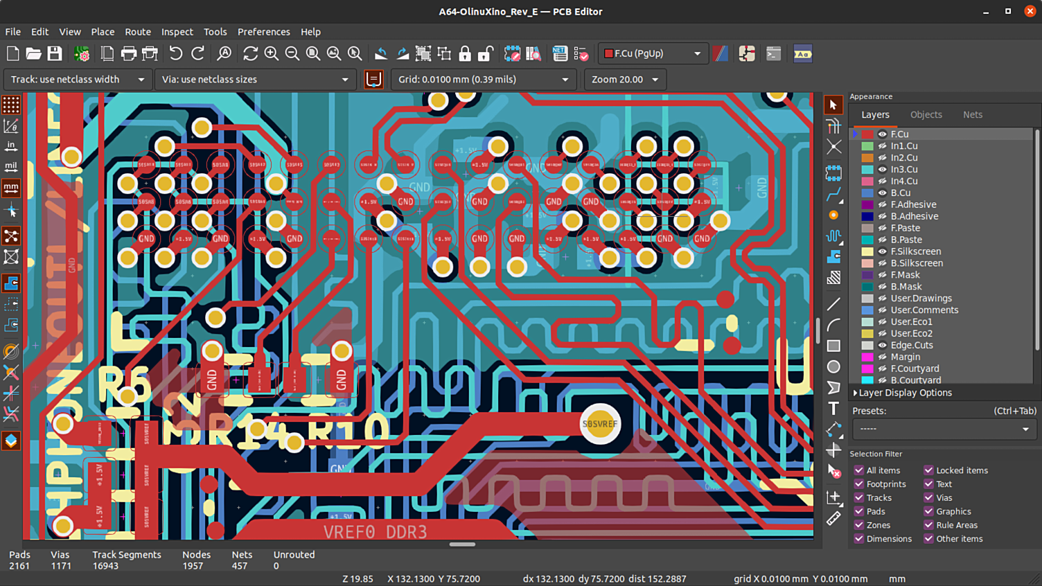
KiCad 8 Custom PCB Design Rules | SaludPCB
 saludpcb.com
KiCad 8 Custom PCB Design Rules | SaludPCB
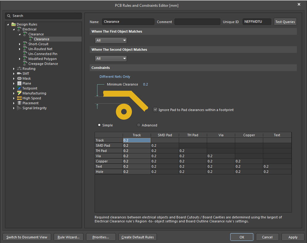
KiCAD-Custom-DRC-Rules-for-JLCPCB-with-Unit-Tests/JLCPCB Rules Test
KiCAD-Custom-DRC-Rules-for-JLCPCB-with-Unit-Tests/JLCPCB Rules Test ...
GitHub - Tomsz1337/ALTIUM_RULES_JLC: Design Rules For Altium Designer
GitHub - Tomsz1337/ALTIUM_RULES_JLC: design rules for altium designer ...
Reglas De Fabricación En KiCAD | Arcos-Lab Wiki
 wiki.arcoslab.org
Reglas de fabricación en KiCAD | Arcos-Lab Wiki
Design Rules For JLCPCB - Manufacturing - KiCad.info Forums
 forum.kicad.info
Design rules for JLCPCB - Manufacturing - KiCad.info Forums
BGA Pad Clearence : R/KiCad
 www.reddit.com
BGA Pad Clearence : r/KiCad
Electrical Design Rule Types Available For PCB Layout In Altium
 www.altium.com
Electrical Design Rule Types Available for PCB Layout in Altium ...
GitHub - Wireddown/jlcpcb-kicad-templates: KiCad Templates For JLCPCB
GitHub - wireddown/jlcpcb-kicad-templates: KiCad Templates for JLCPCB
Defining Rules For A PCB | Altium App StartPage
 my.altium.com
Defining Rules for a PCB | Altium App StartPage
STM32 PCB Design - Complete Walkthrough - Altium Designer & JLCPCB
 www.fedevel.com
STM32 PCB Design - Complete Walkthrough - Altium Designer & JLCPCB ...
RevK®'s Ramblings: JLCPCB And Fun Rules
 www.revk.uk
RevK®'s ramblings: JLCPCB and fun rules
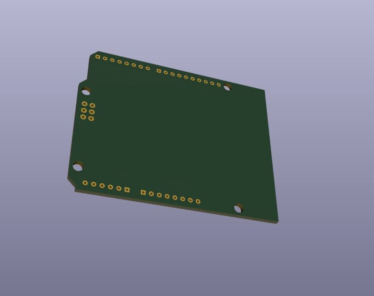
How To Import Altium Designer PCB Board In KiCad? — RefCircuit
 refcircuit.com
How to import Altium Designer PCB board in KiCad? — RefCircuit
KiCad 8 Custom PCB Design Rules | SaludPCB
 saludpcb.com
KiCad 8 Custom PCB Design Rules | SaludPCB
RevK®'s Ramblings: JLCPCB And Fun Rules
 www.revk.uk
RevK®'s ramblings: JLCPCB and fun rules
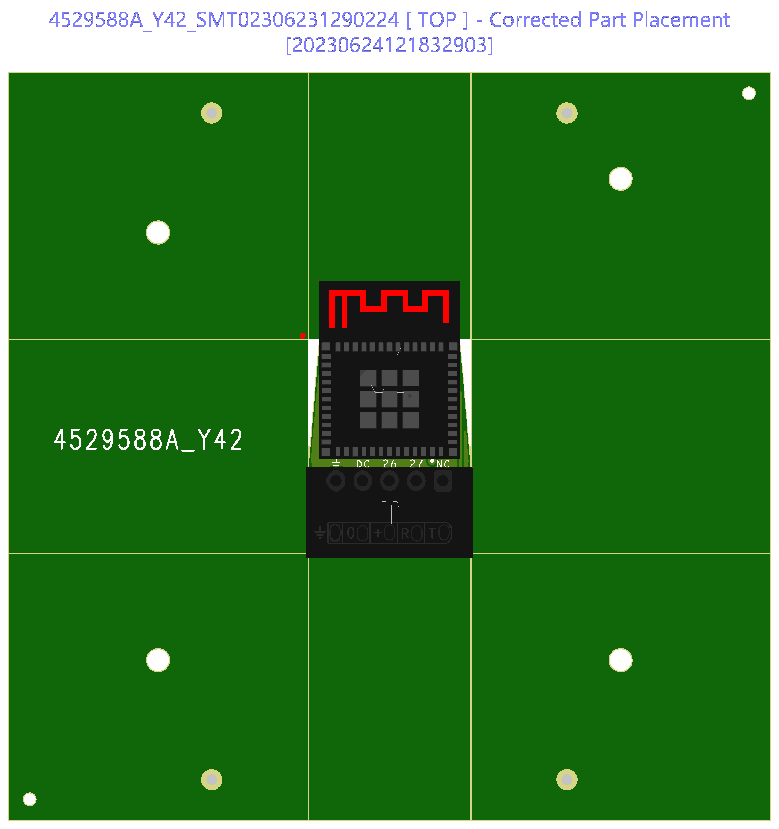
KiCad - JLCPCB, Component Placement Viewer Not Aligned. Anyone Had
 www.reddit.com
KiCad - JLCPCB, component placement viewer not aligned. Anyone had ...
Pcb Design Steps In Kicad - Design Talk
 design.udlvirtual.edu.pe
Pcb Design Steps In Kicad - Design Talk
Module 12: Design Rules - Altium
 www.yumpu.com
Module 12: Design Rules - Altium
KiCad-DesignRules/JLCPCB/JLCPCB.kicad_dru At Main · Labtroll/KiCad
KiCad-DesignRules/JLCPCB/JLCPCB.kicad_dru at main · labtroll/KiCad ...
KiCad - JLCPCB, Component Placement Viewer Not Aligned. Anyone Had
 www.reddit.com
KiCad - JLCPCB, component placement viewer not aligned. Anyone had ...
KiCad - JLCPCB, Component Placement Viewer Not Aligned. Anyone Had
 www.reddit.com
KiCad - JLCPCB, component placement viewer not aligned. Anyone had ...
GitHub - EddyBeaupre/KiCad-JLCPCB-Templates: Templates For 2 And
GitHub - EddyBeaupre/KiCad-JLCPCB-Templates: Templates for 2 and ...
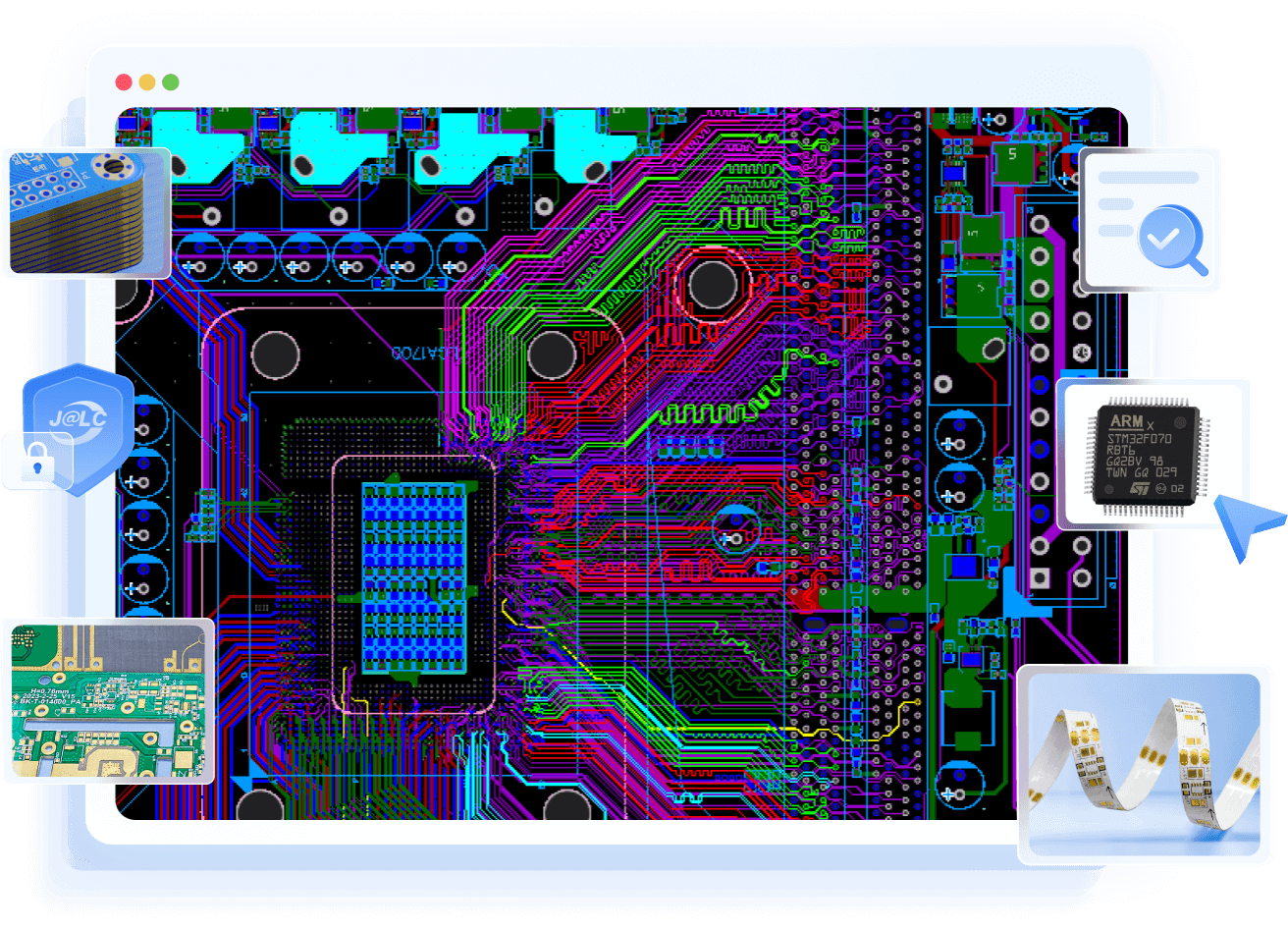
Professional PCB Layout Services | JLCPCB
 design.jlcpcb.com
Professional PCB Layout Services | JLCPCB
Network Graph · MHI-Design/KICAD-Rules-Check-JLCPCB-2-and-4-Layers · GitHub
Network Graph · MHI-Design/KICAD-Rules-Check-JLCPCB-2-and-4-Layers · GitHub
KiCad 8 Custom PCB Design Rules | SaludPCB
 saludpcb.com
KiCad 8 Custom PCB Design Rules | SaludPCB
How To Import Altium PCB Board Into KiCad 7 | SaludPCB
 saludpcb.com
How To Import Altium PCB Board Into KiCad 7 | SaludPCB
Design Pcb And Schematic In Altium, Kicad, Easyeda, And Order From
 www.fiverr.com
Design pcb and schematic in altium, kicad, easyeda, and order from ...
KiCad - JLCPCB, Component Placement Viewer Not Aligned. Anyone Had
 www.reddit.com
KiCad - JLCPCB, component placement viewer not aligned. Anyone had ...
Insanity 4004: JLCPCB Design Rules For Eagle
 insanity4004.blogspot.com
Insanity 4004: JLCPCB design rules for Eagle
RevK®'s Ramblings: JLCPCB And Fun Rules
 www.revk.uk
RevK®'s ramblings: JLCPCB and fun rules
Common Mistakes To Avoid In Electrical Schematic Design | PCB Design Tips
 jlcpcb.com
Common Mistakes to Avoid in Electrical Schematic Design | PCB Design Tips
RevK®'s Ramblings: JLCPCB And Fun Rules
 www.revk.uk
RevK®'s ramblings: JLCPCB and fun rules
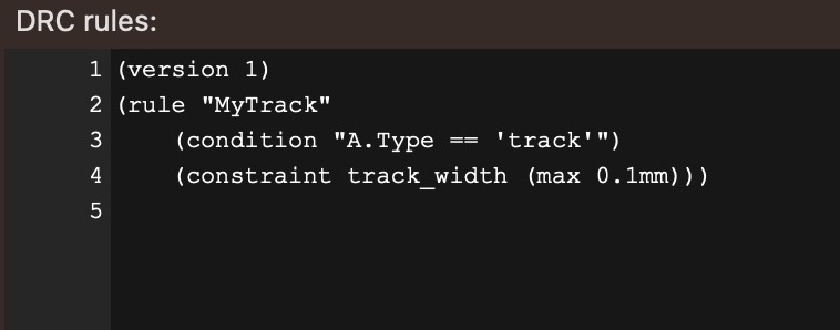
Understanding And Setting Up Design Rules In KiCad
 go.pcbfabexpress.com
Understanding and Setting Up Design Rules in KiCad
Electrical Rule Types | Altium Designer 25 Technical Documentation
 www.altium.com
Electrical Rule Types | Altium Designer 25 Technical Documentation
KiCad Vs. Eagle Vs. Altium - A Comprehensive Comparison For PCB Design
 www.pcba-manufacturers.com
KiCad vs. Eagle vs. Altium - A Comprehensive Comparison for PCB Design ...
How To Fix KiCAD JLCPCB Fabrication Plugin Error: The Wx.App Object
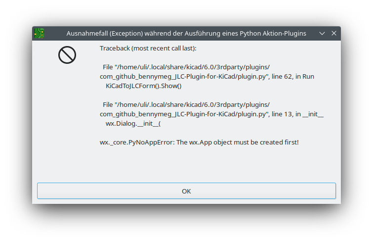 techoverflow.net
How to fix KiCAD JLCPCB fabrication plugin error: The wx.App object ...
Defining rules for a pcb. Revk®'s ramblings: jlcpcb and fun rules. Pcb design steps in kicad